
 首页
首页 登录
登录 注册
注册


HTML
-
The fast development of semiconductor technology in recent decades has dramatically changed the world and improved our life. Semiconductor devices' increasing performance requires to be continually smaller and faster. New materials, such as 2D materials with outstanding electronic and optoelectronic properties, are also pursued to construct new devices with improved characteristics [1-6]. The transport and relaxation of carriers at semiconductor devices' heterojunction, which take place on the nanometer spatial scale and the picosecond to femtosecond time scales, play the key role in determining their functions. These critical small-scale details have attracted a great deal of attention from both experimentalists and theoreticians in both scientific and industrial fields over the past decades. The time-resolved photoemission technique has been very successful in investigating the dynamics of excited electrons on ultrafast time scales. The development of angle-resolved photoemission electron spectroscopy (ARPES) combined with the time-resolved technique has offered additional momentum information, allowing the further understanding of ultrafast electron dynamics [7, 8]. However, due to the lack of spatial resolution in the time-resolved photoelectron spectroscopy, the ultrafast electron dynamics of small samples in micrometer scale has been rarely measured with this method [9-11]. Although the sub-micrometer and even tens of nanometer-scale ARPES has been established by focusing synchrotron lights with Fresnel Zone Plates [12], time-resolved spectroscopy measurements are difficult and achieved only with tens of picoseconds time resolution. In recent years, the development of the time-resolved photoemission electron microscopy (TR-PEEM) technique, which combines ultrafast optics and electron microscopy, provides access to the data needed to make movies of spatiotemporal electron dynamics with high resolution at material interfaces [13-15]. The early applications of TR-PEEM with single-color lasers focused on studies of surface plasmon dynamics [13, 16-18]. This topic is continued to be studied by two-color TR-PEEM [19, 20], which was also used to observe the photo-generated carrier dynamics in GaAs [15, 21]. The PEEM equipped with the energy analyzer offers one more capability to observe details of charge carrier dynamics: the simultaneous evolution of electron density in spatial, temporal and energy domains. Very recently, by using such a 4D spectro-microscopy, Man et al. reported imaging the motion of electrons across the semiconductor heterojunction with unprecedented access to their dynamics [22].
In this work, the setup of the time-resolved spectroscopic PEEM, which we have built up recently, is presented in detail. Its time resolution, electron kinetic energy resolution, and spatial resolution abilities are documented. The results of time-resolved micro-area photoelectron spectra and energy-resolved TR-PEEM images on Pb/Si(111) demonstrate that this setup is a powerful tool to investigate many interesting phenomena in heterojunctions. Examples include the charge transfer and dynamic processes of free carriers, and characterization of novel materials such as size-dependent 2D materials and their heterojunctions.
-
The aberration-corrected spectroscopic photoemission and low energy electron microscopy system (SPELEEM III, ELMITEC GmbH) [23, 24] we used here is located at the XPEEM (X-ray photoemission electron microscopy) endstation of the Dreamline (BL09U) in the Shanghai Synchrotron Radiation Facility (SSRF). FIG. 1(a) shows the electron-optical schematic of the SPELEEM. As a cathode lens electron microscopy, the sample tested in the SPELEEM is held at a high negative potential (
$ - $ 20 kV). Electrons from the sample surface---photoemitted in the PEEM mode or backscattered in the LEEM mode---are collected and accelerated by the objective lens. They then pass through a series of electro-optical elements to produce a magnified image of the sample, with a spatial resolution down to about 6 nm with mercury lamp light and about 16 nm with X-ray source in the PEEM mode, or about 3 nm in the LEEM mode, respectively. The micro-area LEED patterns, which show the surface structure, can be obtained by imaging the back focal plane of the objective lens. The photoelectron diffraction (PED) patterns, with momentum and energy resolution (with energy slit inserted), are also presented in the back focal plane under PEEM to realize micro-area ARPES measurements [25]. The energy dispersive plane of the energy analyzer is imaged by tuning the projector lenses. By inserting the field-limiting aperture in this mode, photoelectron spectra of surface micro areas (10, 5, or 1.5 μm in diameter) can be acquired with the energy resolution of about 150 meV, whereas through inserting energy slits in the dispersive plane in the imaging mode, spectro-microscopy within a narrow kinetic energy window down to about 0.2 eV can be realized for a specific energy range. Thus, element-specific or element chemical state-specific images can be acquired with the synchrotron X-ray as the light source.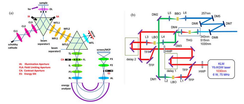
We very recently combined the ultrafast laser with the SPELEEM to achieve the femtosecond time-resolved spectroscopic PEEM test results. FIG. 1(b) shows a schematic of the pump-probe laser path for the TR-PEEM. An oscillator (FLINT, Light Conversion) delivers 6 W with a pulse width of less than 100 fs, at the wavelength of 1030 nm and at the repetition rate of 76 MHz. A true zero-order half-wave plate and a thin film polarizer are used to distribute the laser power to the pump and probe lasers paths. The pump laser, i.e. the second order harmonic (SH) 515 nm (2.4 eV) is generated by focusing the fundamental harmonic within a lithium triborate (LBO) crystal, and the third order harmonic 343 nm (3.6 eV) is generated by mixing the fundamental and SH within a
$ \beta $ -barium borate (BBO) crystal. The fundamental harmonic can also be provided as a pumping laser with some optics removed. The probe laser, fourth order harmonic (FH) at 257.5 nm (4.8 eV), is generated by doubling the SH within a thin BBO crystal. This FH photon energy is larger than the work functions of most materials needed to induce single-photon photoemission. The pump and probe lasers are collimated with a customized dichroic mirror (DM8 in FIG. 1(a)), and then focused by using an uncoated lens with the focus length 150 mm in front of the fused silica window of the PEEM chamber. Both pump and probe lasers are collinearly focused on the sample at an angle of about 16$ ^\circ $ relative to the sample surface, and their sizes on the sample are optimized by finely tuning the collimation lens after the nonlinear crystals. All of the measurements in this work were carried out at room temperature. The sample temperatures were raised by about 15$ - $ 30 K by the laser illumination.
-
The temporal resolution was measured by the cross-correlation of the second harmonic (515 nm) and the fourth harmonic (257.5 nm) pulses. A boron doped Si(111) substrate (
$ \rho $ $ < $ 0.005$ \Omega\cdot $ cm) with a natively oxidized surface, which has a high work function value, was used to measure non-resonant two-photon photoemission. The pump pulse (515 nm) was focused on an area of about 40 μm$ \times $ 70 μm, and the probe pulse (257.5 nm) was focused on an area of about 100 μm$ \times $ 200 μm. The photoelectrons generated by the pump-probe were collected by the PEEM, to produce an image showing the locally different photoemission intensities. The TR-PEEM image series can be obtained by scanning the time delays ($ \Delta t $ ) between pump and probe pulses.The TR-PEEM images were recorded using a delay step of 13 fs. FIG. 2(a)-(c) show TR-PEEM images for
$ \Delta t $ =$ - $ 400 fs (i.e., for a probe pulse arriving at 400 fs earlier than the pump pulse), 0, and 94 fs, respectively. FIG. 2(d) is the PEEM intensity versus$ \Delta t $ , averaged over the circle region, as marked in FIG. 2(b). Fitting of a Gaussian line shape gives a full width at half maximum (FWHM) of 184 fs, which defines the time resolution of this equipment. The temporal resolution is mainly limited by the pulse width of the laser output and the nonlinear crystal thickness for both of the second and forth harmonic generation. It can be seen that almost no signal is visible when the two pulses have no temporal overlap or the probe pulse is earlier than the pump pulse. The signal gradually increases with a partial timing-overlap, and reaches its maximum with full overlap between the two pulses. FIG. 2(d) also shows subsequent carrier dynamics with longer time delays, which are attributed to the surface photovoltaic (SPV) effect [15].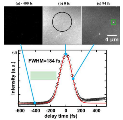
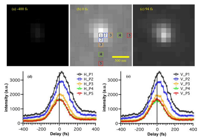
In FIG. 2(a)-(c), there are some bright spots with higher photoelectron yield than surrounding areas. These are assumed to be nanoscale structures with lower work functions or more electronic states [21]. One of them is marked out with green square in FIG. 2(c). This green square zone is magnified to show pixel-resolvable (about 150 nm/pixel) images of different delay times in FIG. 3(a)-(c) with the same gray scaling. As shown in FIG. 3(b) of zero delay time, pixel-1 (P1) has the highest intensity of the bright spot. Four other pixels, P2 to P5, are also chosen in both horizontal (H) and vertical (V) directions respectively, which are at different distances from P1. Time-resolved PEEM intensity profiles collected from these pixels are plotted in FIG. 3(d) and (e). Apparently, the peaks of the intensity curves for the pixel H-P5 in FIG. 3(d) and V-P5 in FIG. 3(e), far away from the pixel P1, appear earlier than that for the pixels closer to P1. This must be attributed to the specific electron dynamics of such an nanoscale structure distinct from that of the surrounding areas. Among all the experiments in this work, we have not tested the spatial resolution limit of our instrument in time-resolved measurements. The above result shows that at least the intensity/dynamics discrepancies in space as fine as 150 nm can be discriminated. Further time-resolved measurements with high spatial resolution will be done in future work.
-
The structures and energetics of the interfaces between metals and semiconductors are crucial in both fundamental and technological fields. In semiconductor devices, interfaces with metal electrodes play an important role in the functionality of the devices. Examples include integrated circuits, photovoltaic cells, and light-emitting diodes. Silicon, as the most commonly used semiconductor, has been thoroughly investigated with various metal adsorbates. These form a variety of interface structures. The quantum well states of epitaxial Pb thin films on Si(111), a nearly ideal quasi-2D model system, have been intensively studied in the electron structures and ultrafast electron dynamics of all the occupied, unoccupied and interface states in the past [26-30]. Here, the electron dynamics of Pb islands in the small spatial scale on Si(111) as a test example has been studied on the ultrafast time scale. The functions of our new setup were fully demonstrated with this system.
The Pb islands were grown in situ on the Si(111)-7
$ \times $ 7 surfaces at room temperature with a prototype evaporator under ultrahigh vacuum condition (base pressure$ < $ 2$ \times $ 10$ ^{-10} $ mbar). The surface of the Si(111) with the 7$ \times $ 7 reconstruction was prepared by repeatedly flashing the substrate to about 1400 K. The Pb grows on Si(111)-7$ \times $ 7 surfaces in the Stranski-Krastanov mode, with a wetting layer and the subsequent formation of islands. The pump laser power is about 114 mW, and the probe laser power is about 1 mW. The power of both pulses was finely tuned to avoid any space charge effect, which can induce image distortion and broaden photoelectron spectra for some materials with high photoelectron yield. Here, the laser-based photoemission with low kinetic energies benefits enhanced bulk sensitivity [31], which allows the detection of interface states at the buried interface for thin films. FIG. 4(a) shows a PEEM image of an as-grown Pb island. Some diffraction fringes can be observed beside its edges under the laser illumination, due to the light diffraction [32, 33]. Electrons photoemitted from the blue circle area (5 μm in diameter) on the Pb island were selected by the field-limiting aperture, and the photoelectron spectra were recorded in the dispersive plane imaging mode. The micro-area time-resolved photoelectron spectra are plotted in FIG. 4(b). The$ X $ axis represents the relative kinetic energy of the photoelectrons, which was not calibrated. Seven photoelectron spectra, marked in black in FIG. 4(b), are selected from the delay series and replotted in FIG. 4(c) for closer comparison. The photoelectron spectra show two features of the kinetic energy. Before the time overlap, both the lower and higher energy features decrease in intensity over time delay. After the time overlap, the lower energy feature falls further, and the higher energy one rises. After the excitation delay of about 10 ps, the spectrum is almost fully recovered. Moreover, it also obviously shows that the photoelectron spectrum moves to the left even when the probe pulse is about 2 ps before the pump pulse. However, it seems only the low energy sides of the spectra move with delay time, while the high energy sides remain the same. Hence, it does not originate from SPV effect, which shows a shift of the whole spectrum. Comparing the experimental results to that reported in Ref.[34], the pumping power density of less than 0.5$ μ $ J/cm$ ^2 $ in our experiment is too low to generate a measurable SPV. We tentatively attribute the interesting phenomenon observed here to the charge transfer across the Pb/Si interface. This charge transfer must induce photovoltaic effect, similar to SPV. The reason why this has not been observed might be caused by the partial electrical field shielding from the Pb island. To elucidate its dynamics thoroughly, further investigations will be carried out with Pb islands of different thicknesses and sizes.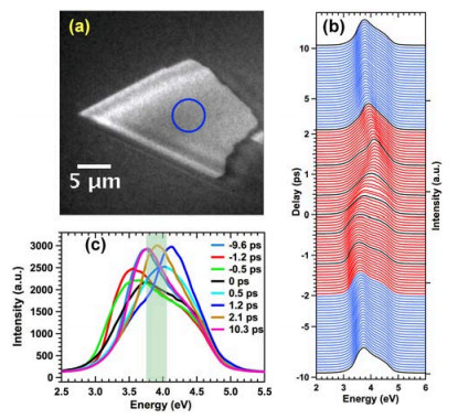
Time-resolved spectro-microscopy images of the Pb island were recorded by selecting electrons within the energy window of 0.3 eV as marked with the gray bar in FIG. 4(c). FIG. 5(a-e) correspond to the obtained images at different time delays of
$ - $ 9.6,$ - $ 0.82, 0, 2 and 10.3 ps, respectively. A reference image taken at$ - $ 18.3 ps, FIG. 5(f), has been subtracted to present the changes more clearly. We find that the intensity of the Pb island changes obviously with the time delay. The intensity at around time of zero is quite weak, and the highest intensity appears at about 2 ps. Two areas, one blue rectangle and one red circle, as shown in FIG. 5(f), are selected on the Pb island to plot their average intensities with respect to the delay time in FIG. 5(g). Both curves show that the intensities decrease before the time overlap and increase after it, and there is an obvious dip at about 1 ps. Comparing the images for different time delays, the intensity changes at the island edge facing the incident laser are more pronounced than the center of the island. The difference might come from different photo-generated carrier population and relaxation processes. The intensity profile that occurs along the black solid line in FIG. 5(f) is plotted in FIG. 5(h). This shows the intensity oscillations induced by the diffraction field beside the island edge. In this measurement, a lateral resolution of 220 nm is roughly estimated from the diffraction fringes. Further studies are necessary to understand the mechanism of the position-dependent dynamics. The spectro-microscopy imaging can supply us more clues to help infer the relaxation of exited carriers, in terms of both the energy distribution and the spatial distribution.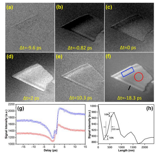
-
We constructed an ultrafast time-resolved spectroscopic PEEM for studying the carrier dynamics of the heterojunctions. This instrument is composed of a femtosecond time-resolved laser system and a spectroscopic PEEM. It allows us to study the evolution of electrons in space, time, and energy, representing 4D spectro-microscopy. The temporal resolution was determined to be 184 fs, by measuring the cross-correlation of the pump (515 nm) and the probe (257.5 nm) pulses on the SiO
$ _2 $ /Si surface. The spatial resolution in the above experiments was 150 nm or better, and the resolution limit of TR-PEEM imaging was not deliberately tested. The time-resolved micro-area (5 μm) photoelectron spectra on Pb/Si(111) show a complicated dynamic process, and the TR-PEEM at specific kinetic energy shows highly position-dependent dynamics. These encouraging results suggest that the instrument is a powerful tool to investigate ultrafast carrier dynamics in submicron or even nanometer scale in semiconductor heterojunctions.
-
This work was conducted at the XPEEM endstation (BL09U, Dreamline) in the Shanghai Synchrotron Radiation Facility. This work was supported by the National Key R & D Program (No.2018YFA0208700 and No.2016YFA0200602), the National Natural Science Foundation of China (No.21688102 and No.21403222), the Strategic Priority Research Program of the Chinese Academy of Sciences (No.XDB17000000), and the Youth Innovation Promotion Association of Chinese Academy of Sciences (No.2017224).
 DownLoad: